About Our Ion Implantation Services ABOUT
Nissin Ion Equipment Co., Ltd. provides high-quality ion implantation services powered by our own state-of-the-art, in-house developed ion implanters. We support a wide range of applications, from cutting-edge 300 mm silicon devices to advanced power semiconductors and optoelectronic devices, including:
• High-temperature ion implantation for SiC and GaN devices
• Hydrogen ion implantation for VCSEL applications
• Implantation for small-diameter wafers and small samples
All processes are performed in a Class 1 clean environment, equivalent to our customers’ LSI production lines, ensuring the highest level of process cleanliness and reliability.
We also have ion beam etching equipment and provide etching processing services.
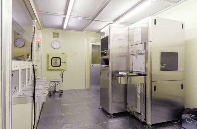
In addition to this, we offer comprehensive evaluation capabilities, including annealing, sheet resistance measurement, dose monitoring, and particle inspection. This integrated environment allows us to support process development, device evaluation, and early-stage R&D, especially for advanced technology nodes.
We invite you to leverage our ion implantation expertise to accelerate your device development.
Fields Served by Our Ion Implantation Services
Silicon devices
High-precision, high-purity ion implantation
SiC, GaN, and Ga₂O₃ power devices
Al⁺, Si⁺, and Mg⁺ implantation
High-temperature implantation up to 600°C possible
GaN and SiC Smart Cut wafers
Wafer stripping through high-concentration hydrogen implantation
VCSEL (Vertical cavity surface emitting LASER)
High-energy hydrogen implantation
Cutting-edge process development
Support for new device architectures and novel processes using specialty ion species.
IBE (Ion Beam Etching) / Ion Milling
Dry etching by noble gas ion (Ar⁺) beam irradiation
Why Choose Nissin? MERIT
High-quality implantation services
- Access to state-of-the-art ion implantation technology developed by an ion implanter manufacturer
- Support for 300 mm wafers and advanced implantation processes
- Processing in a Class 1 clean tunnel environment
- Ideal for advanced node device development and experimental processes
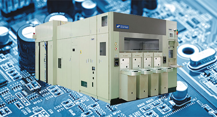
EXCEED Series – Key Benefits
- Parallel beam architecture
- Beam parallelism controllable to ±0.5 deg or better
- Pre-implantation uniformity verification
- Complete elimination of energy contamination
- FOUP load port for 300 mm wafers
The end station is directly connected to the clean tunnel, enabling ion implantation in a Class 1 clean environment.
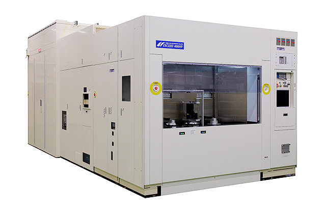
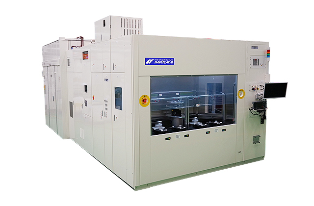
IMPHEAT-II – Key Benefits
- Wafer temperatures up to 500 ℃
- Aluminum ion implantation
- Designed for power device applications
- Parallel beam architecture
- Beam parallelism controllable to ±0.5 deg or better
- Pre-implantation uniformity verification
Complete elimination of energy contamination
Implantable Ion Species
Our 8-inch wafer implanter supports a wide variety of ion species, beyond those typically available on mass-production semiconductor lines. This capability is ideal for:
• Research and development of new devices
• Process feasibility studies
• Contamination and reliability evaluations
●: Implantable Ion Species
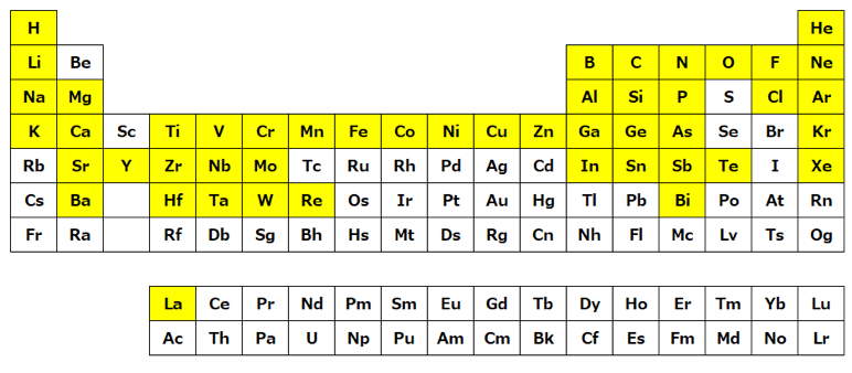
Ion species not listed may also be available using our KYOKA material modification system. Please contact us to discuss your specific requirements.
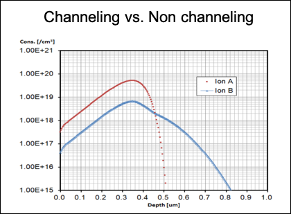
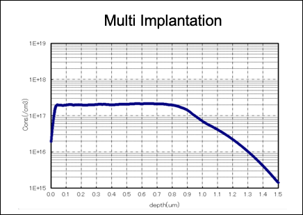
Ion Implantation Simulations
To meet precise process requirements, we offer ion implantation simulations that optimize:
• Ion species
• Implantation depth
• Concentration profiles
• Channeling vs. non-channeling conditions
• Multi-implant strategies
These simulations help ensure that the proposed process achieves the desired dopant distribution before actual implantation.
From Development to Production Support
Whether you are:
• Exploring a new device concept
• Optimizing a critical implantation step
• Preparing for mass production
Nissin’s ion implantation services provide the process accuracy, flexibility, and technical depth needed to move forward with confidence.