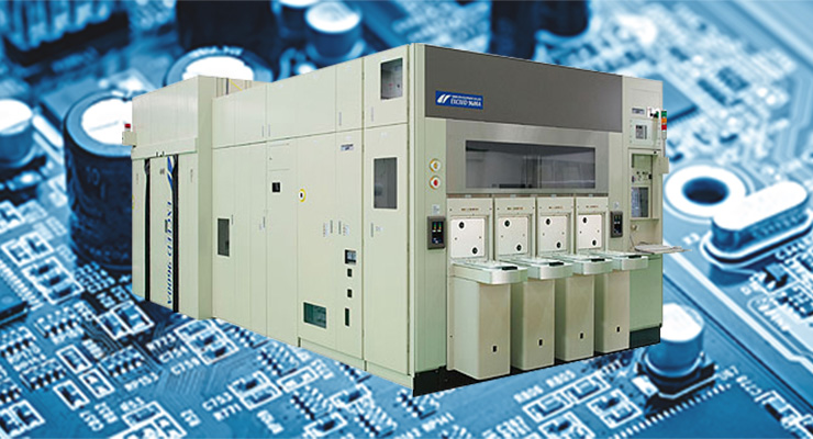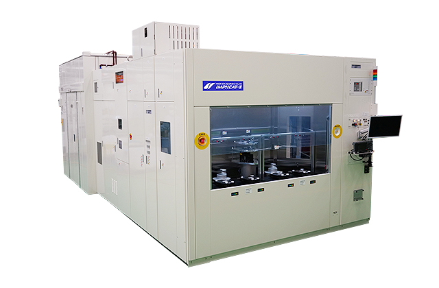
What Is Ion Implantation?
Ever since first transistor was invented at Bell Laboratories in 1947, semiconductors have become incredibly advanced, to the benefit of industrial development. In the future as well, semiconductors will play a central role in industry, being used for electronic device control, automobile electrification, the automation of industrial equipment using ICT (information and communication technology), and even the advancement of digital transformation (DX) and IoT. Ion implantation plays an important role in a wide variety of complex processes used for manufacturing semiconductor products. In recent years, the ion implantation process has become increasingly important particularly for manufacturing power devices, which have been a focus of attention for their use in automotive semiconductor products.
The ion implantation process alters the electrical properties of a substrate, which starts out as a non-conductor, by implanting impurities that act as donors or acceptors, turning it into a usable semiconductor. This process plays an indispensable and extremely important role in the processes for manufacturing semiconductor and FPD(Flat Panel Display). In the illustration in figure 1, the sponge is the non-conductive substrate, and the baseballs are impurities that become donors or acceptors.
The semiconductor manufacturing process can be divided into two major parts: the front-end process and the back-end process. The FPD manufacturing process also consists of two parts: the array process and the color filter–cell–module process.
Ion implantation, together with the photoresist coating, exposure and development, etching, photoresist stripping/cleaning, and planarization steps, is positioned as part of the processes referred to as the front-end process and array process. These processes are repeated numerous times with different circuit patterns to form electronic devices as shown in the cross-section diagram in Figure 2.
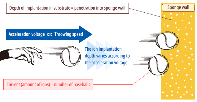
Figure 1
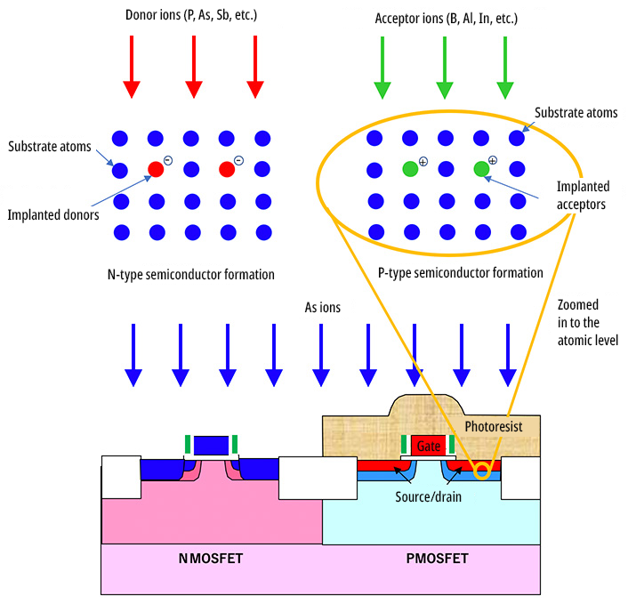
Figure 2. Example of ion implantation as part of the semiconductor manufacturing process
(NMOS source/drain forming process)
Fields Expected to Benefit in the Future
Ion beam technology is expected to be applicable to a variety of fields, including medicine, space, energy, and novel materials.
The spread of power devices to more EVs and high-speed trains

The proliferation of AR/VR displays and transparent displays
Integration technology for fusing different materials through exfoliation bonding (hydrogen/helium implantation)
Ultrafine processing technology based on surface modification (low-energy, high-current implantation)
Automated equipment operation and monitoring technology based on artificial intelligence

Bringing Together Diverse Cutting-Edge Technologies
The equipment technologies that make these technologies possible involve a wide variety of technical fields.
For example, a group of engineers with expertise in vacuum technology, electronic circuit technology, plasma chemistry, materials engineering, high-voltage insulation technology, mechatronics, telecommunications, IT, and so on are working to develop equipment and process technology with the aim of commercializing products in new application fields.