Material Modification
This technique uses large quantities of ions to impart new functionality to material and realize processing that was previously impossible. As semiconductor device structures have been becoming more and more complex and approaching the physical limits, existing fabrication processes alone are not enough to step further. Material modification is expected to be a breakthrough in the semiconductor manufacturing process.
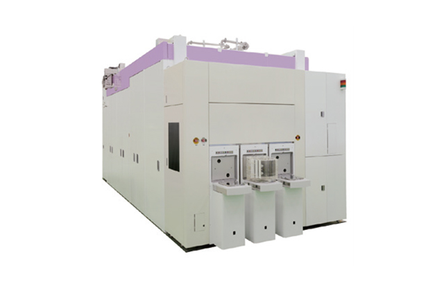
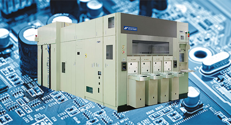
To change material properties, large amounts of ions are generally irradiated at low energies, which results in several atomic percent in the material. For this reason, mass production is not feasible with ordinary ion implantation equipment due to low productivity and requires dedicated material modification equipment which can generate high current ion beam.
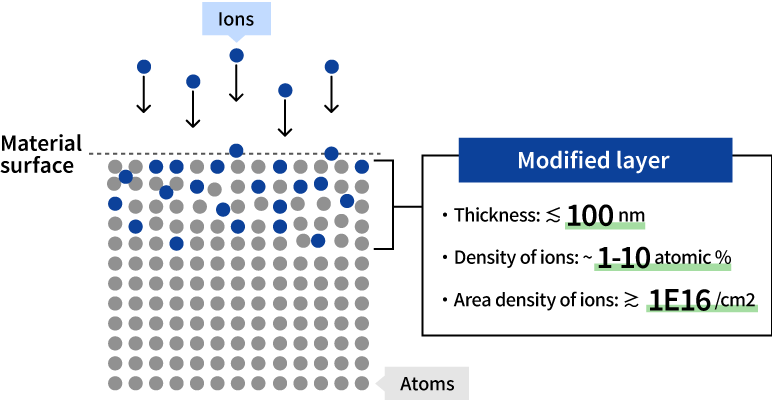
Schematic diagram of material modification
Effect of material modification
The effects and applications of material modification technique are diverse. The following examples have been reported.
Etching rate control
Etching rate can be altered with ion irradiation. This improves etching selectivity between different materials. You can change both dry and wet etching rates. Furthermore, this technique can control the depth of the modified layer. When the layer is modified to be etch-resistant, etching stops there. In other words, it is possible to form an etch-stop layer at a preferred depth.
CMP (chemical mechanical polishing) rate control
CMP removal rate can be changed with ion irradiation. This enhances the CMP selectivity of different materials existing on the polishing plane. Irradiating only the outer edge of wafers allows to change the rate locally. You can slow down the removal rate only at the edge. This helps to cancel out the higher rate at the edge than the center, which is general in CMP process, and improve the uniformity across the wafer.
Mask hardening
Ion irradiation can make masks more etch-resistant. This technique is effective for both organic and inorganic masks. it allows use of masks thinner than usual and suppresses the mask pattern collapse. In addition, the hardened masks keep their original shape during etching, which facilitates more precise deep etching processes.
Area selective deposition
Ion irradiation can render material surface inactive so that no film grows on the irradiated area during a subsequent deposition process. When trench patterns are irradiated, only the top and bottom are deactivated as ion beam is directional. Subsequent deposition creates a structure in which the film is deposited only on the trench sidewalls.
Stress formation
Implanting ions into material forms stress in it. This can be used to solve the problem of wafer warpage that has become apparent in recent years as the film layers on the wafer become thicker. Creating stress on the backside surface compensates warpage and flattens the bowed wafer without affecting semiconductor devices on the front surface.
Thin film peeling
High dose hydrogen ion implantation at a certain depth from the surface splits the material at the implanted layer after thermal treatment. Patterned masks allow localized peel-off. A structure with the thin layer on a supporting substrate can be obtained when the irradiated surface is bonded to the substrate then split.
Gate threshold voltage (Vth) control
The process of forming CMOS with high-k materials and metal gates is complex. One method is to create dummy gates, form the source and drain, remove the dummy gates, and embed the metal gates, but this step must be repeated twice because the gate materials are different for pMOS and nMOS. On the other hand, ion implantation can modify the metal gate’s threshold voltage so that the same material can be used for both and the voltage for each gate can be independently fine-tuned to what it should be. This approach has a potential to simplify the complex process and reduce the cost.
Directional deposition
Irradiation of many ions which is directional enables directional deposition. When this technique is applied to trench patterns, a film doesn’t grow on trench sidewalls but top and bottom.