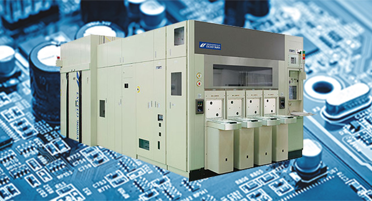
Ion implanter for FPD manufacturing
iG6 Ver.2
We provide ion implanters that are indispensable for the electrical characteristics control process in the manufacture of thin-film transistors for driving high-definition displays, as typified by low-temperature polysilicon thin-film transistors.
We provide ion implanters that are indispensable for the electrical characteristics control process in the manufacture of thin-film transistors for driving high-definition displays, as typified by low-temperature polysilicon thin-film transistors.
Merit
- High equipment reliability as recognized at mass production plants around the world
- A single implanter unit can handle a variety of dopants and a wide implantation range (channels and source/drain regions).
- High precision and high reproducibility are achieved by our proprietary high-precision ion beam measurement system and high-precision glass substrate scanning mechanism.
- Rapid switching between different dopant recipes using proprietary technology
- High-purity implantation through proprietary technology for mass separation impurity removal
- Suppression of glass substrate temperature increases during implantation by means of a dual platen mechanism
- Mitigation of glass substrate charging (electrostatic discharge damage) during implantation by means of a charge neutralization system
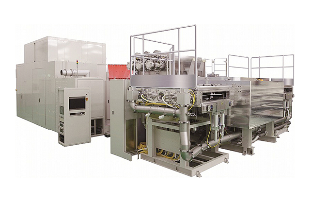
Main Specifications
Available glass substrate sizes
1,500 mm x 1,800 mm
Dopants (ion species)
B+、P+
Ion beam energy
10–80 keV
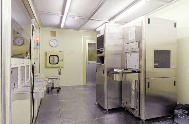
Track Record
Delivered to display panel manufacturers and laboratories in Japan, China, South Korea, and Taiwan.
Implanter available compatible for 6th-generation glass substrates: IG6, IG6 Ver. 2 (100% global market share, according to internal study)
Delivered to display panel manufacturers and laboratories in Japan, China, South Korea, and Taiwan.
Implanter available compatible for 6th-generation glass substrates: IG6, IG6 Ver. 2 (100% global market share, according to internal study)