We’ve developed a machine that enables mass production of the semiconductor material modification process.
SHIGA, Japan – Nissin Ion Equipment Co., Ltd. (hereinafter referred to as Nissin Ion Equipment) has developed a new semiconductor material modification machine called KYOKA that is capable of mass production in the material modification process that plays a part in the manufacture of semiconductor devices.
KYOKA was designed by applying the company’s high-current ion technology developed for smartphone display manufacturing—a market dominated by Nissin Ion Equipment—and is the world’s first machine that satisfies all the various performance requirements for practical application and mass production of material modification, including high throughput and low processing cost. In April 2024, a demonstration machine will be installed at Nissin Ion Equipment’s Shiga Plant to begin processing samples for customers.
Nissin Ion Equipment is pursuing six growth strategies under Vision 2025, the company’s medium-to-long-term business plan for the Nisshin Electric Group. This project is one of the corporate activities that will contribute toward “expansion of environmentally friendly products.”
Our customers are eager to introduce new processes that will enable further advancements in the miniaturization of semiconductors, including artificial intelligence (AI) chips that are a hot topic of late and expected to make significant contributions to the future development of science and technology, as well as the lower power consumption and more advanced functionality that smaller-scale semiconductors will offer. One such process is the use of ions to modify materials. By using low-energy ion beams to irradiate the materials from which semiconductor devices are made, such as silicon and silicon oxide, we can impart properties not present in the original materials. However, this process requires an extremely large volume of ions, and conventional machines have been unable to satisfy the productivity and cost requirements, which has been a major obstacle to practical applications of this process.
Development on the new KYOKA began in 2017 and was prompted by feedback from customers who wanted a machine capable of material modification for mass production. Through simulation-based analysis of ion beam trajectories and a series of mechanical, electrical, and software design improvements, we succeeded at developing a machine with mass production performance that could satisfy the market’s needs. In addition to improving the functionality of the material itself, this machine also modifies the properties of the material in order to facilitate the subsequent semiconductor fabrication process, contributing both to improved device performance and to the advancement of manufacturing technology.
This article is based on results obtained from a project (JPNP 21009) commissioned by the New Energy and Industrial Technology Development Organization (NEDO).At Nissin Ion Equipment, we will continue to contribute to our customers’ development and the achievement of a sustainable society as the first company to deliver innovative manufacturing equipment that the world needs.
[Features of KYOKA]
1. High processing performance
KYOKA is capable of high-throughput material modification processing at a rate of 25 wafers or more per hour, achieving a three-fold productivity boost compared to conventional equipment.
2. A wide range of processing regions
KYOKA can also be used for material modification processes that require low-energy regions under 1 keV through the use of ultra-high-current ion beams. This expands the range of material modifications that KYOKA can be applied to.
3. Compatibility with diverse material modification processes
A variety of ion species can be generated to achieve optimal modification in accordance with the target material.
4. Compatibility with cutting-edge semiconductor manufacturing lines
KYOKA can handle 300-mm wafers and is suitable for use on cutting-edge semiconductor manufacturing lines.
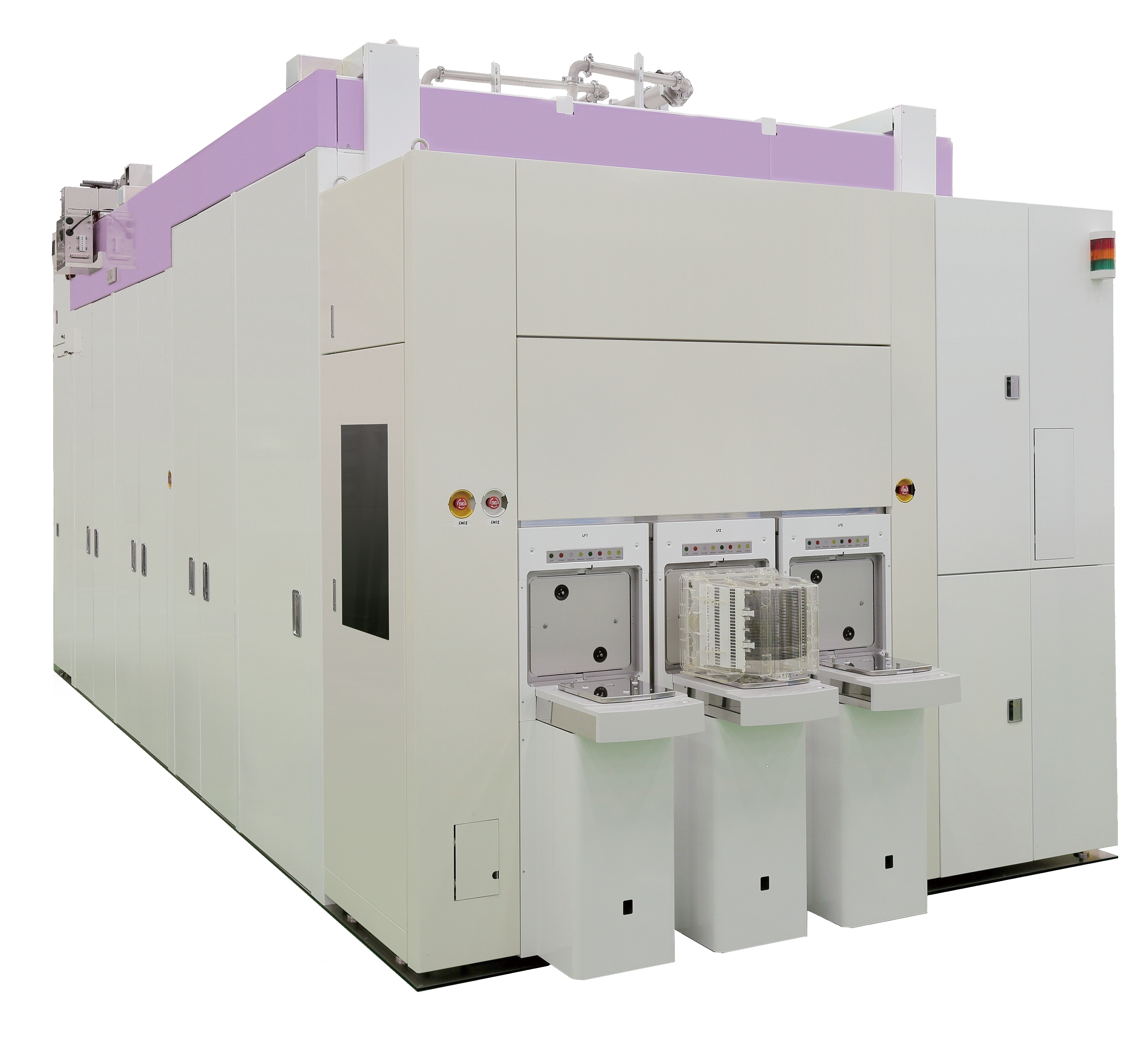
The Newly Developed KYOKA
KYOKA will be exhibited through display panels and videos at SEMICON Japan 2023, an international trade show for semiconductor manufacturing equipment and materials (organized by Semiconductor Equipment and Materials International [SEMI]), which will be held at the Tokyo Big Sight from Wednesday, December 13 to Friday, December 15.
Nissin Ion Equipment has been stepping up its efforts to promote the SDGs through its business operations. This accomplishment is related to the following goals among the 17 SDGs.
7. Affordable and Clean Energy
9. Industry, Innovation and Infrastructure
■Contact information related to KYOKA:
Contact us Semiconductor Material Modification Machine_KYOKA
Reference
Explanation of Terms:
• Semiconductor material modification machine
This is a device that can modify the properties of materials used in semiconductor manufacturing. There are a variety of methods for making these modifications. One of them is to irradiate the material with ions.
• Six growth strategies
Environmentally friendly products, response to distributed energy, response to renewable energy, adoption of DX to products and business, identifying demand resulting from increasing environmental awareness in emerging countries, business expansion in association with the expansion of EVs.
• High throughput
This refers to a high processing volume for a given unit of time. This is one of the most basic performance requirements for manufacturing equipment.
• New Energy and Industrial Technology Development Organization (NEDO)
NEDO is a national research and development agency created to foster innovation through the advancement of technology development required to achieve a sustainable society.
• Semiconductor Equipment and Materials International (SEMI)
SEMI is an organization that promotes the growth of semiconductor manufacturing and supply chain companies around the world.
• SEMICON Japan
SEMICON Japan is an international trade show for the semiconductor manufacturing supply chain that is organized by SEMI’s Japanese branch. It includes seminars and networking events.